components
Hardware Components
X 1
Software Apps and online services
details
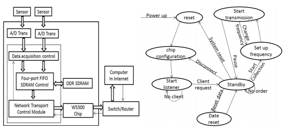
Analysis the overall structure and the hardware design of new data acquisition system. This system take FPGA as the main chip, and control multi-channel AD chip to collect data. This work eventually use the Cyclone II family EP2C70F672C8N chip as the main chip to achieve, relative to other design which uses such as DSP and ARM microprocessor, internal control circuit is simple and reliable, and has more power and cost advantages. Data transmission could through switches and routers to achieve the data collection and transmission of any distance, at LAN conditions, the maximum data rate can reach 80Mbps.
For more detail, go to https://www.sciencedirect.com/science/article/pii/S2212667812001220
documents
Code
Schematics
Others
COMMENTS