
Original Link: https://www.researchgate.net/publication/332577041_FPGA_based_Multichannel_Bit_Error_Rate_Tester_for_Spacecraft_Data_Acquisition_System
Its a research paper , in this paper for this project they have used WIZnet 5300 (Ethernet Controller) and it is used for communication between FPGA and PC with an application.
Bit Error Rate (BER) is a principle measure of data transmission link performance. BER tester (BERT) consists of a Pattern Generator and an Analyzer that can be set to the same pattern. The payload data transmitted from the spacecraft consists of one, two or three channels per carrier based on the modulation scheme. The traditional equipments can do BER analysis for only one channel at a time. In order to support multichannel BER analysis, a Personal Computer (PC) based system is designed and implemented in Altera Stratix II (EP2S130F1508C5N) FPGA. Ethernet is configured using WIZnet 5300 (Ethernet Controller) and it is used for communication between FPGA and PC with an application. Application is used to transmit the Pattern Generator’s configurations from PC to FPGA and to receive Analyzer’s status. Packet processing is done for this communication using User Datagram protocol (UDP). On the whole, traditional equipments are replaced by the designed and implemented bit error rate tester.

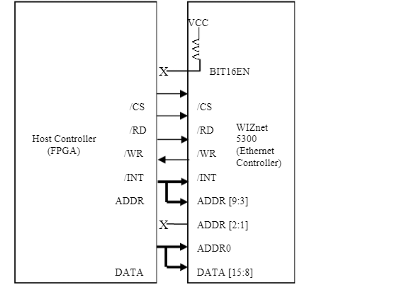
WIZnet 5300 (Ethernet Controller)
In this Ethernet controller memory is extended to 128Kbyte and 16 bit bus interface is supported. It
consists of eight hardware sockets which can be used simultaneously. In this project only one is used.
Communication can be established using Protocols such as Transmission Control Protocol (TCP), User
Datagram Protocol (UDP), IPRAW and MACRAW. TCP is a connection-oriented protocol. UDP is a
connection-less protocol. UDP supports unicast, broadcast and multicast methods. In this project UDP
(unicast method) is used [6]. Socket status transition for UDP (Unicast method) and UDP operation flow are
shown in figure 5 and 6 respectively.
Direct addressing mode is implemented. For 16bit data bus width, ADDR [9:1] is used and ADDR0
is connected to ground or floated. ‘BIT16EN’ is internally pulled-up, so it is no problem if it is allowed to
float. The connections are shown in figure

COMMENTS