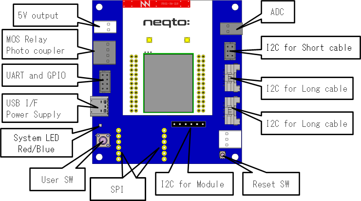
NEQTO Bridge Digital IO Board
Overview
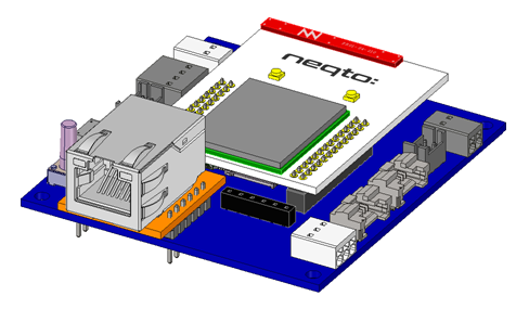
The NEQTO Bridge Digital IO Board is an evaluation extension board for easily connecting peripheral devices to the peripheral interface of the NEQTO Bridge Module, such as UART, SPI, I2C, and GPIO.
Hereinafter, “NEQTO Bridge Digital IO Board” is called “IO board” and “NEQTO Bridge Module” is called “module”.
By identifying the connected IO board, the module automatically enables the function unique to the IO board.
neqto.js’ nqEx Object is used to control each interface. All interfaces are disabled by default, so enable them as needed.
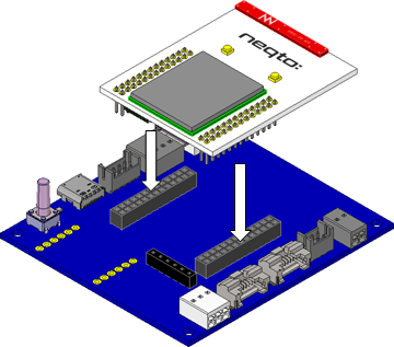
For information regarding the “Method for inserting and removing a module”, refer here.
Main Specifications
| Item | Specs | Notes |
|---|---|---|
| Digital I/O | UART x 1 ch SPI x 1 ch I2C for Module x 1 ch I2C for Short cable x 1 ch I2C for Long cable x 2 ch GPIO x 2 ch | |
| Photo Coupler Input | 1 ch | Refer to the module specifications. |
| MOS Relay Output | 1 ch | Refer to the module specifications. |
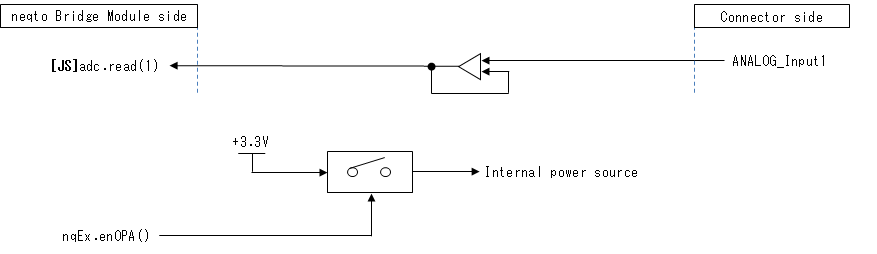
| Analog Input | 1 ch OPA365 is used as a non-inverting buffer for ADC. | Common-mode voltage range:min 0.1 V, max 3.2V@3.3 V |
| Reset SW | 1 ch | |
| User SW | 1 ch | |
| LED | 2 LEDs | System LED1 (Red), System LED2 (Blue) |
| USB | USB 2.0 Full Speed compatible 4.75 V – 5.25 V | – 2 A@5 V recommended – USB Type-C™ compliant connector |
| 5V Output | 1 ch | Current Limit: 0.5A |
| Operating Temperature Conditions | 0 ℃ – 50 ℃ | |
| Storage Temperature Conditions | 0 ℃ – 50 ℃ | |
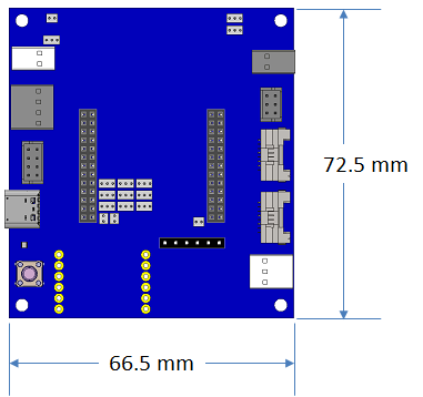
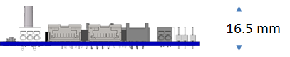
| Size | 66.5 mm x 72.5 mm x 16.5 mm |
External Dimensions
Interfaces
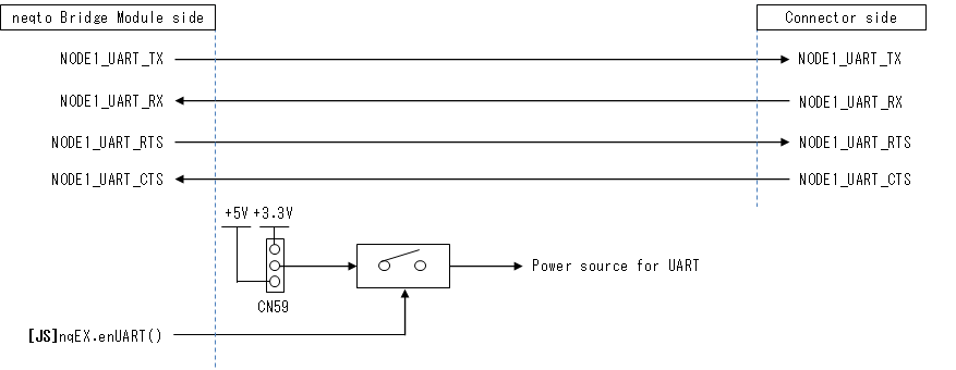
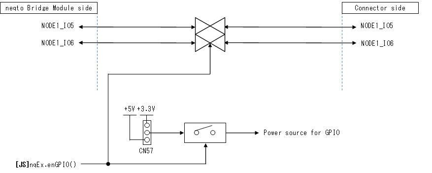
UART / GPIO
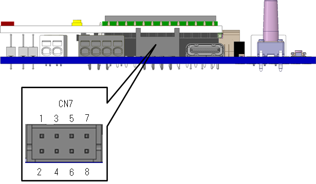
| Pin No. | Signal Name | Note |
|---|---|---|
| 1 | VDD_UART | 3.3V / 5V |
| 2 | GND | Ground |
| 3 | NODE1_UART_TX | NEQTO Output |
| 4 | NODE1_UART_RX | NEQTO Input |
| 5 | NODE1_UART_RTS | NEQTO Output |
| 6 | NODE1_UART_CTS | NEQTO Input |
| 7 | NODE1_IO5 | NODE1_IO5 |
| 8 | NODE1_IO6 | NODE1_IO6 |
Block diagram
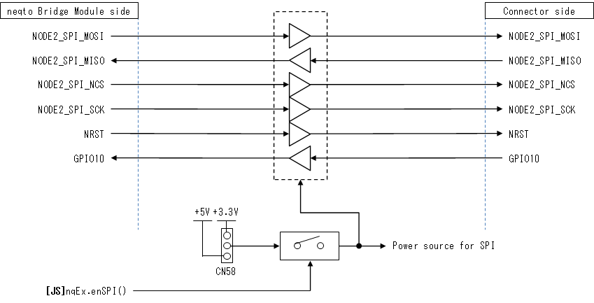
SPI
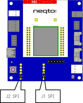
J1 terminal
| Pin No. | Signal Name | Note |
|---|---|---|
| 1 | GND | Ground |
| 2 | GND | Ground |
| 3 | NODE2_SPI_MOSI | NEQTO Output |
| 4 | NODE2_SPI_SCK | NEQTO Output |
| 5 | NODE2_SPI_NCS | NEQTO Output |
| 6 | GPIO10 | NEQTO Input The SPI port must be enabled to use this pin. This input pin is pulled up externally with 10kΩ and should be used in GPIO operation mode 0(IN/PULL-UP) or 2(IN). |
J2 terminal
| Pin No. | Signal Name | Note |
|---|---|---|
| 1 | GND | Ground |
| 2 | VDD_SPI | 3.3V / 5V |
| 3 | VDD_SPI | 3.3V / 5V |
| 4 | Reserved | Not Connect |
| 5 | NRST | NEQTO Output The SPI port must be enabled to use this pin. The NRST signal is output. Not Connect when not in use. |
| 6 | NODE2_SPI_MISO | NEQTO Input |
Block diagram
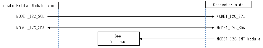
I2C for Module
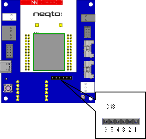
| Pin No. | Signal Name | Note |
|---|---|---|
| 1 | VDD+3V3 | |
| 2 | GND | Ground |
| 3 | NODE1_I2C_SDA | |
| 4 | NODE1_I2C_SCL | |
| 5 | NODE1_I2C_INT_Module | |
| 6 | Reserved | Not Connect |
Block diagram
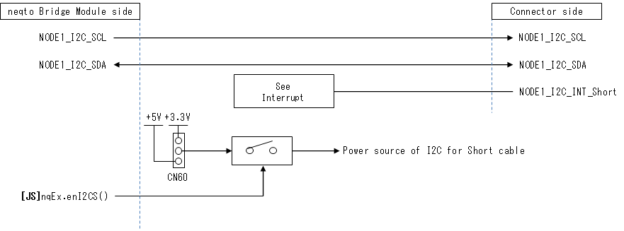
I2C for Short cable
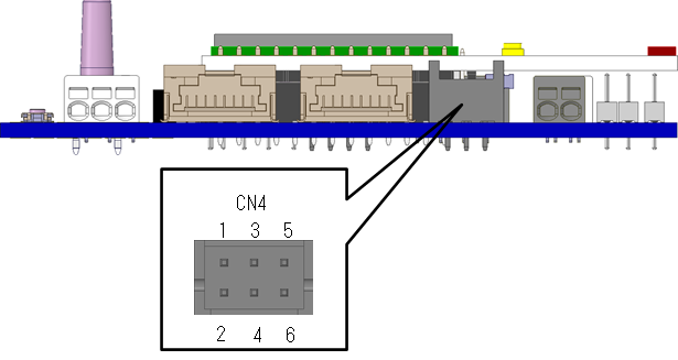
| Pin No. | Signal Name | Note |
|---|---|---|
| 1 | VDD_I2CS | 3.3V / 5V |
| 2 | GND | Ground |
| 3 | NODE1_I2C_SDA | |
| 4 | NODE1_I2C_SCL | |
| 5 | NODE1_I2C_INT_Short | |
| 6 | Reserved | Not Connect |
Block diagram
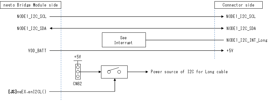
I2C for Long cable
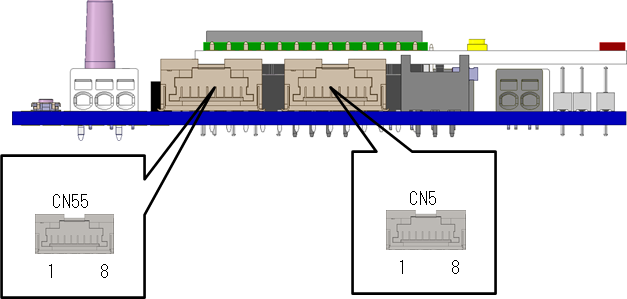
| Pin No. | Signal Name | Note |
|---|---|---|
| 1 | VDD_I2CL | 5V |
| 2 | NODE1_I2C_SDA | |
| 3 | GND | Ground |
| 4 | NODE1_I2C_SCL | |
| 5 | GND | Ground |
| 6 | NODE1_I2C_INT_Long | |
| 7 | GND | Ground |
| 8 | Reserved | Not Connect |
Block diagram
Interrupt
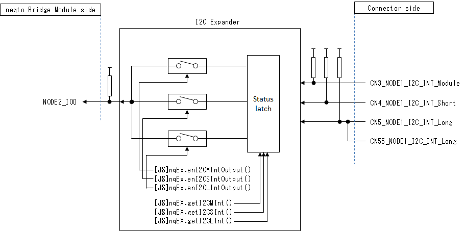
The each NODE1_I2C_INT signal output to I2C Expander must be active low and open drain output.
The interrupt signal output signal of I2C Expander (NODE2_IO0) is active low and open drain output.
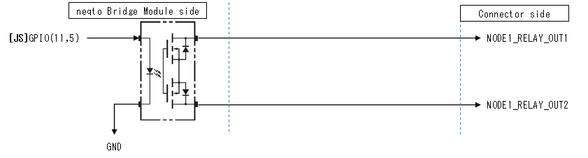
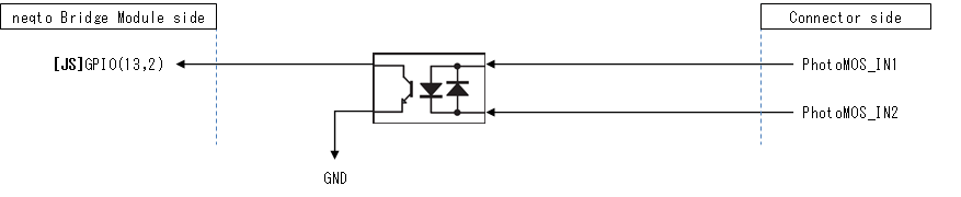
MOS Relay / Photo Coupler
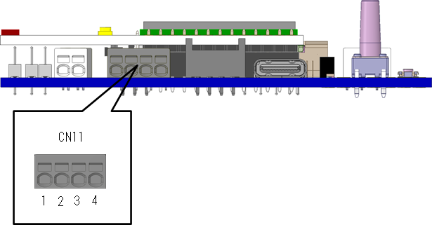
| Pin No. | Signal Name | Note |
|---|---|---|
| 1 | NODE1_RELAY_OUT1 | |
| 2 | NODE1_RELAY_OUT2 | |
| 3 | NODE1_PhotoMOS_IN1 | |
| 4 | NODE1_PhotoMOS_IN2 |
Block diagram
ADC
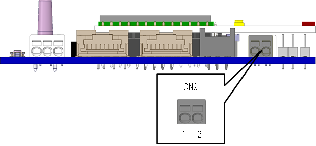
| Pin No. | Signal Name | Note |
|---|---|---|
| 1 | ANALOG_Input1 | ADC Input |
| 2 | GND | Ground |
Block diagram
External Power Output
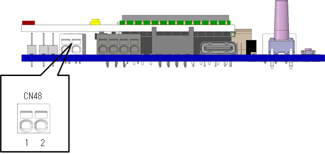
| Pin No. | Signal Name | Note |
|---|---|---|
| 1 | External Power Output | 5V |
| 2 | GND | Ground |
Interface Specifications
| Item | Spec | Notes |
|---|---|---|
| Low Level Input Voltage 1 | Max 0.8 V@VDDSEL = 3.3 V(Note 1) | UART / SPI/ GPIO |
| Low Level Input Voltage 2 | Max 0.9 V@VDDSEL = 3.3 V(Note 1) | I2C for Module |
| Low Level Input Voltage 3 | Max 2 V@VDDSEL = 5.0 V(Note 1) | I2C for Long cable |
| Low Level Input Voltage 4 | Max 0.15 V@VDDSEL = 3.3 V(Note 1) | I2C for Short cable |
| High Level Input Voltage 1 | Min 2.0 V@VDDSEL = 3.3 V(Note 1) | UART / SPI / GPIO |
| High Level Input Voltage 2 | Min 2.35 V@VDDSEL = 3.3 V(Note 1) | I2C for Module |
| High Level Input Voltage 3 | Min 2.8 V@VDDSEL = 5.0 V(Note 1) | I2C for Long cable |
| High Level Input Voltage 4 | Min 2.9 V@VDDSEL = 3.3 V(Note 1) | I2C for Short cable |
| Low Level Output Voltage 1 | Max 0.6 V@IOL = 24 mA VDDSEL = 3.3 V(Note 1) | UART / SPI / GPIO |
| Low Level Output Voltage 2 | Max 0.5 V@IOL = 4 mA VDDSEL = 3.3 V(Note 1) | I2C for Module |
| Low Level Output Voltage 3 | Max 0.5 V@IOL = 1 mA VDDSEL = 3.3 V(Note 1) | I2C for Short cable |
| High Level Output Voltage 1 | Min 2.35 V@IOH = 24 mA VDDSEL = 3.3 V(Note 1) | UART / SPI / GPIO |
| High Level Output Voltage 2 | Min 2.8 V@IOH = 4 mA VDDSEL = 3.3 V(Note 1) | I2C for Module |
| High Level Output Voltage 3 | Min 2.2 V@IOH = 20 μA @VDDSEL = 3.3 V(Note 1) | I2C for Short cable |
| Output Voltage | open-collector Max 5 V 330 Ω pull-up | I2C for Long cable |
- Note 1) VDDSEL
When 3.3V is selected: It is supplied from RP601Z330A.
The output deviation of RP601Z330A in the PWM / VFM automatic switching method is 3.3 V -2% + 4%.
When 5V is selected: Supplied by TPS61372.
The output deviation of the TPS61372 is 5.0 V ± 5%@PWM.
Short Plug
CN10 / CN61
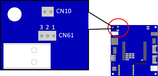
| CN No. | Function | Configuration |
|---|---|---|
| CN10 | Photo Coupler Input pull-up setting | Open: No pull-up resistor (default)Close: 2.2 kΩ resistance to pull-up to 3.3 V |
| CN61 | Output voltage setting for CN48 | 1-2: Do not use 2-3: 5V (default) |
CN60 / CN62
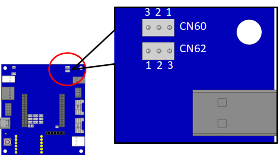
| CN No. | Function | Configuration |
|---|---|---|
| CN60 | Output voltage setting for VDD_I2CS | 1-2: 3.3V 2-3: 5V |
| CN62 | Output voltage setting for VDD_I2CL | 1-2: 5V (default)2-3: Do not use |
CN50 / CN51 / CN53 / CN54 / CN57 / CN58 / CN59 / CN63 / CN64 / CN65 / CN66
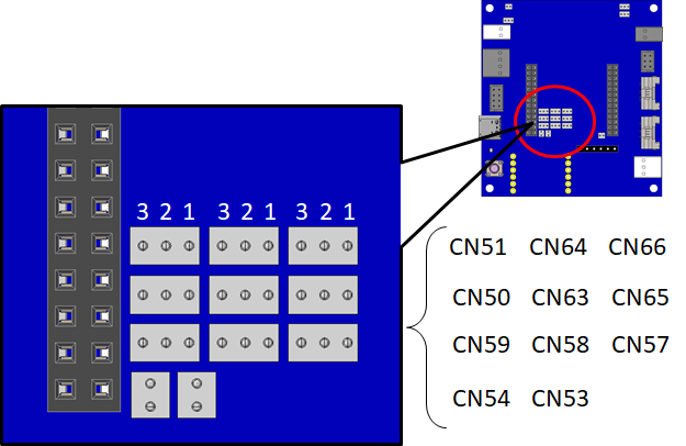
| CN No. | Function | Configuration |
|---|---|---|
| CN50 | Signal setting connected to CN7_5 pin | 1-2: Do not use 2-3: NODE1_UART_RTS (default) |
| CN51 | Signal setting connected to CN7_6 pin | 1-2: Do not use 2-3: NODE1_UART_CTS (default) |
| CN53 | Serial signal setting when using User Console mode | Open: Do not use Close: (default) |
| CN54 | Serial signal setting when using User Console mode | Open: Do not use Close: (default) |
| CN57 | Output voltage setting for VDD_GPIO | 1-2: 3.3V (default)2-3: 5V |
| CN58 | Output voltage setting for VDD_SPI | 1-2: 3.3V (default)2-3: 5V |
| CN59 | Output voltage setting for VDD_UART | 1-2: 3.3V (default)2-3: 5V |
| CN63 | Signal setting connected to CN7_3 pin *CN66 setting is also required. | 1-2: NODE1_UART_TX (default)2-3: RS-232C level data transmission |
| CN64 | Signal setting connected to CN7_4 pin *CN65 setting is also required. | 1-2: NODE1_UART_RX (default)2-3: RS-232C level data reception |
| CN65 | Signal setting connected to CN7_4 pin *CN64 setting is also required. | 1-2: RS-232C level reception data 2-3: NODE1_UART_RX (default) |
| CN66 | Signal setting connected to CN7_3 pin *CN63 setting is also required. | 1-2: RS-232C level transmission data 2-3: NODE1_UART_TX (default) |
CN43
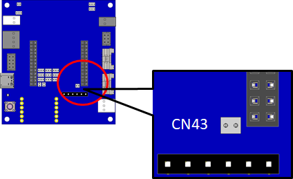
| CN No. | Function | Configuration |
|---|---|---|
| CN43 | Reserved | Open: (default)Close: Do not use |
Connector List
| Function | Address | Parts Number | Maker | Socket | Crimp terminal | Maker |
|---|---|---|---|---|---|---|
| UART, GPIO | CN7 | DF11-8DP-2DSA | Hirose Electric | DF11-8DS-2C | DF11-2428SCA | Hirose Electric |
| SPI | J1, J2 | Through hole | ||||
| I2C for Module | CN3 | FSS-41035-06 | Hirosugi Keiki | PSS-410153-06 | Hirosugi keiki | |
| I2C for Short cable | CN4 | DF11-6DP-2DSA | Hirose Electric | DF11-6DS-2C | DF11-2428SCA | Hirose Electric |
| I2C for Long cable | CN5, CN55 | DF50A-8P-1H | Hirose Electric | DF50A-8S-1C | DF50-2830SCFA | Hirose Electric |
| Photo Coupler Input, MOS Relay Output | CN11 | 1770908 | Phoenix Contact | |||
| Analog Input | CN9 | 1702473 | Phoenix Contact | |||
| External Power Output | CN48 | 1814498 | Phoenix Contact | |||
| Battery | CN41 | 1814508 | Phoenix Contact | |||
| USB | CN44 | CX90B1-24P | Hirose Electric | |||
| NEQTO Bridge Module | CN1, CN2 | FSS-22043-13 | Hirosugi Keiki |
Appendix
LAN Module installation
By connecting an Ethernet module with an RJ-45 connector, it can be used in a wired network environment. Please contact us for more information.
Ethernet module model number: WIZ850io
COMMENTS