IOTA Crypto Core FPGA — 4th Progress Report
This is my 4th progress report. In case you missed the 3rd: link

The third milestone has been finished!

I was asked a lot to give an ELI5 about the project. So I try :)
What is an FPGA?
FPGA is an abbreviation for “Field Programmable Gate Array”. Digital logic can be described in a hardware description language like VHDL or Verilog and synthesis-Tools can synthesize digital hardware out of these descriptions.
You could see it this way: CPUs are executing programs. An FPGA can be configured to run e.g. CPUs which execute programs :)
FPGAs often are used for prototyping hardware which could later be used for manufacturing ASICs (real chips). ASICs are a lot faster and need less energy but they are immensely expensive to manufacture (6 digit amount). And if something changed — for instance a new hashing algorithm — the chip would have to be manufactured completely new.
FPGAs easily can be reconfigured because the configuration is volatile. With every power-up cycle the configuration is loaded into the FPGA again. Many FPGAs also support encryption. That means, the configuration can be encrypted and the FPGA would only accept configurations which can be decrypted by decryption keys stored (volatile or permanent) inside the FPGA. This can be used as copy-protection or protection against tampering or analysis of the configuration.
What is the FPGA module?
Whereas in the second milestone the FPGA-core (configuration) for the FPGA was developed, this milestone was about developing an FPGA module which uses the FPGA-core.
Both combined together could be seen as Secure Crypto Processor with hardware acceleration for algorithms used a lot in IOTA.
Following a size-comparison of the module with a 1EUR coin.

Secure Processors are not new — for instance ST Micro has some which also are used on the Nano Ledger Wallet. Often they have dedicated hardware which speed up calculations of e.g. SHA256 or ECDSA significantly — but there is no Secure Processor which has support for algorithms used in IOTA.
This is where the FPGA core + module comes into play. It’s like a Secure Processor but with support for algorithms used in IOTA.
It can do the following:
- integrated Cortex M1 (32Bit ARM with 100MHz clock) which is programmable in C/C++. It also can be debugged via a standard debugging interface (SWD).
- it has accelerators for Trinary <-> Binary type conversions, Hashing (CURL-P81, KECCAC384, Troika; single clock-cycle per hashing-round) and can do Proof-of-Work very fast (~330ms avg).
- it does Seed management and can store up to 8 seeds in a secure memory
- it provides a JSON-Api which can be used via RS232. Currently it offers commands, for generating Addresses or random Seeds, signing Transactions and PoW — everything hardware accelerated.
- everything runs contained in the FPGA and the configuration file of the FPGA can be encrypted. It’s very easy to update the FPGA configuration but it’s impossible* to tamper with the microprocessor-code (which is embedded as ROM) or to extract sensitive information like keys.
- it has integrated peripherals like RS232 or SPI and digital inputs and outputs which are routed to the module-connector and offers spare (unused) pins at the upper side of the module.
*: There is no “impossible” when it comes to security. But the encryption algorithm AES128 is unbroken.
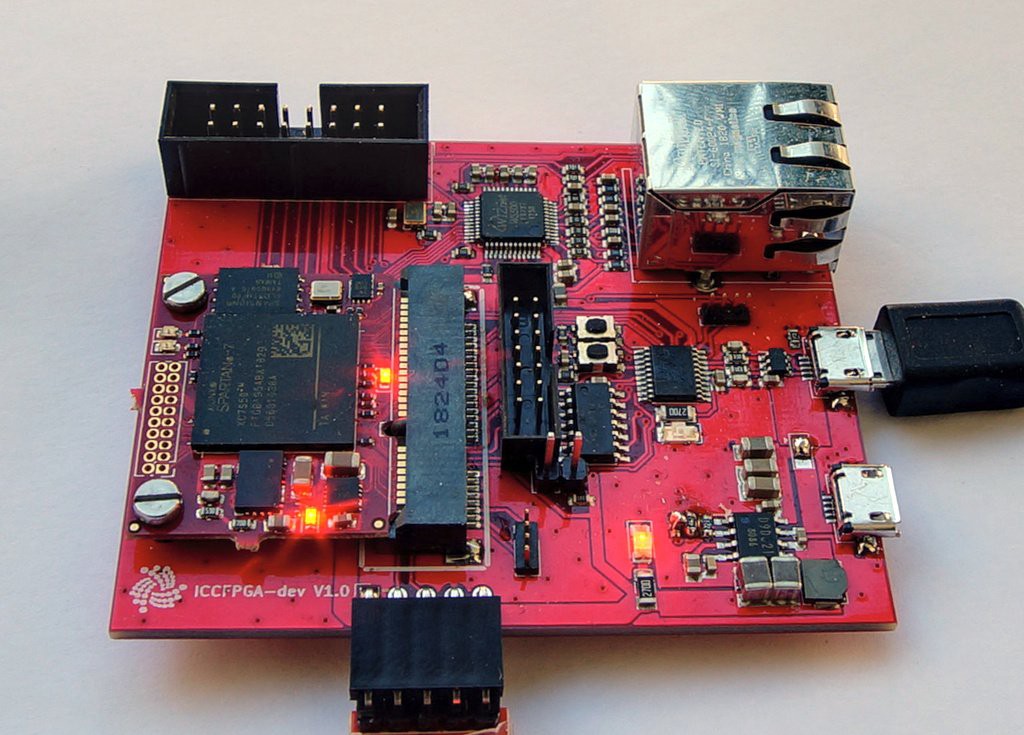
Additionally, a “dev”-board (for testing the module and trying out some things) was developed. On the following picture, you can see the FPGA-module (which is 30x26mm in size) on the left side. The bigger board is the “dev”-Board.

In it’s current state, the FPGA-module together with the board already could run stand-alone applications. It has an ethernet chip for communicating with a LAN network (with e.g. IOTA Full-Nodes). Prior tests showed that the performance is high enough to submit PoWed value bundles to the tangle with about 1TPS (PoWed bundle with 3 TX; 1 Input with Security Level 2 Signature, 1 Output). Unfortunately the Full-Node API-Call “getTransactionsToApprove” needs about 3-4s alone. But the problem of gTTA performance is known and it certainly will be improved in the near future.
Documentation and Code
The main-project documentation (which has been updated and extended with end of milestone 3) can be found here: https://gitlab.com/iccfpga/iccfpga-core/wikis/home
All Repositories are grouped together here: https://gitlab.com/iccfpga
What’s next?
The next milestone is about developing a Linux System-on-Module which will use the FPGA module as Secure Crypto processor :)
This will be even more challenging than the FPGA module. I hope it will work.
Thank you again for reading this much text :)
COMMENTS