1. Introduction
Increasing the reliability and keeping the economical aspect at low levels are one of the upcoming trends in the field of a high voltage power machinery maintenance. Investments into the diagnostic processes could be returned rapidly, especially when these steps avoid cost-ineffective repairs. Periodical inspection together with the correct data representation are the key approaches to increase lifetime cycle of the high voltage machinery. Nowadays there are several diagnostic methods widely used. Basically, they can be divided into two groups, first are
invasive methods and second, more effective, non-invasive. Invasive methods have large limitations and they can not be used for on-line or periodic testing on-site. On the other hand
the non-invasive methods could be used directly on particular place without uncomfortable moving. The main advantage is in the fact that non-invasive testing could be done several times in regular cycles at the same device under test (DUT). These steps allow to compare results from all tests from past months or even years. Diagnostics could be further divided to the electrical based and non-electrical, where no additional testing voltage is connected and the devices are inspected in a different way. Acoustic and mechanical testing could be performed in addition to the classical electrical testing to achieve more accurate results.
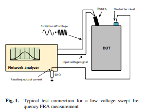
2. Traditional Impulse Method
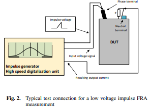
In contrast with the previous method the impulse method tries to compensate several imperfections of the swept mode. Basic principal is described in [1] and especially in [3]. Measurement is done in a frequency domain with single impulse transition response analysis. Test connection for the impulse measurement is shown in Fig. 2. Network analyser is altered by the impulse generator with a high speed digitalization unit. Main idea behind this measurement is to produce a single low voltage impulse to one terminal of the DUT and measure particular response to this impulse on the neutral terminal. Similarly the current on the neutral terminal should be properly converted to the voltage. There is a possibility to use another value of the sensing
impedance in contrast with internal one in the network analyser. Once the time domain record of the voltage (input) and current (output) are recorded, the transfer function is calculated as the Fast Fourier Transform (FFT) of the output divided by the FFT of the input. Unfortunately this method has also its limitation.
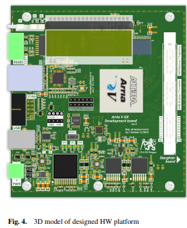
3.1. FPGA board
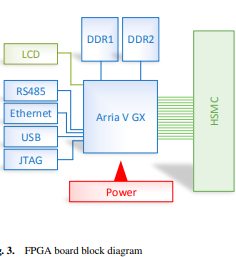
Core parts of the digital subsystems are placed on the field-programmable gate array (FPGA) board. Block diagram is shown in Fig. 3. To obtain easy implementation of real-time parallel tasks and large scalability the FPGA architecture was chosen. Altera Arria V GX device in FBGA672 case [8] provides reasonable ratio between requested functionality and price. Two memory interface for DDR3, large amount of internal RAM and high speed GPIO interfaces are the essential parts.

3.2. Analog front-end board
The analog conversion front-end board connects via HSMC connector. The high speed ADC part consists of ADS42LB69 from Texas Instruments which provides 16- bit conversion at a maximum rate of 250 MSPs. According to [9] the connection with the FPGA is done via LVDS DDR (double date rate) or QDR (quad data rate) interleaving mode. Both possibilities could be used due to versatile PCB design. Analog inputs are prepared for a signal in range up to 2 Vpp. Signal conditioning is prepared for both AC or DC coupling.
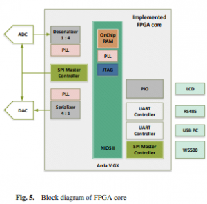
3.3. Implemented FPGA software
Block diagram of implemented FPGA core is in Fig. 5. Data handling from the high-speed ADC is done with a deserialization circuit of quad-data-rate (QDR) data interface. This part is supported with dedicated phase-lockedloop (PLL). Due to serialization factor of 1:4 the effective data rate is 400 Mbit/s. This throughput must be handled precisely with the designed FPGA circuits in VHDL. Serialization circuit for DAC3282 is shown at the left side.
3.4. System preliminary tests
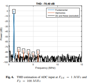
Completely manufactured and assembled digital FPGA board is the main result of this work. Besides the hardware design the FPGA core was programmed to perform basic tasks. All peripherals on the board had been tested with VHDL code blocks and C code firmware block inside SoC NIOS 2. Hardware acts like local-are-network (LAN) node and reacts to the TCP communication port which is available for data exchange and control commands. Data throughput via TCP connection is about 10 Mbit/s. High speed data conversion is done inside VHDL and user is able to acquire 16-bit wide samples from dual channel input in Fs = 100 MSP s. Sampling of the 1 MHz sine wave signal with FS = 100 MHz has been done as one of the preliminary tests. THD value of the obtained data are shown in Fig. 6.
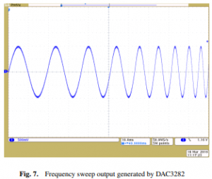
DAC output was tested with a basic sine-wave frequency sweep from 50 Hz up to several kHz. Amplitude of the output voltage is 2 Vpp. Measured waveform is in Fig. 7. Sampling frequency was 20 MHz.
4. Conclusion
This paper dealt with the design of the hardware platform for frequency response analysis (FRA) testing for noninvasive diagnostic purposes. Widely used diagnostic methods has been described in the beginning with special emphasis on the frequency response analysis FRA method. Designed FPGA core has been proposed according to the identified requirements. Full schematic and layout design together with manufacturing, assembling and software testing has been done consequently. Excitation front-end board and further testing on real objects will be the main topic of the future work.
COMMENTS