I. INTRODUCTION
The ever-increasing quantity of data moving around the datacenter and over the Internet is straining the infrastructure as it struggles to keep up. Core functions such as the storage sub systems, the data switches and routers, and even the computing systems are now I/O limited. External data movement is limited by how fast and how far data can move through the cables
and other interconnects that tie all the switches, routers, and storage arrays together. Hence in order to monitor the real time data of certain measurement control system, it is necessary to establish a data transmission system between host computer and measurement control system.
II. THE PROPOSED METHOD
The measurement control system transmits some random data to the host computer through the data transmission system. The flow of data is as follows:
The data of measurement control system is sent over the fiber optic cable.
This is received by optical transceiver of data transmission system. Then the data is sent to FPGA through external PHY chip DP83640 and wiznet W5300 chip.
From FPGA the data is transmitted to host computer through wiznet module.

A. System Performance Requirements
For Optical fiber transmission, the transmission rate is around 100 Mbps of selected optical transceiver. In order to communicate with Optical fiber, the optical fiber interface is achieved using external physical layer (PHY) chip DP83640.
B. System Architecture
The data transmission system is the bridge between the measurement control system and the host computer. The data coming from the measurement control system can be the random
pre trigger signals of some detectors. The data is sent to the data transmission system via fiber optic and then it is sent to the host computer via the Ethernet after the data transmission system receives it.
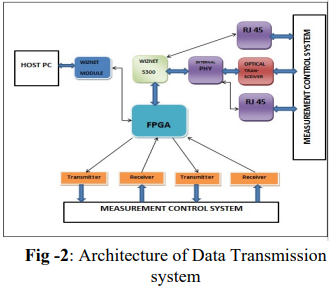
C. System Hardware Architecture
The hardware structure of data transmission system includes optical fiber data transceiver part, Ethernet module for interfacing with host computer, the control unit FPGA and the power
supply system. The optical transceiver is divided into the photoelectric conversion part and data encoding/decoding part. The special media interface chip is required for interfacing optical
transceiver. This is achieved through media interface chip DP83640 Precision Phyter (External Physical Layer).
III. COMPONENT SELECTION
The various major components used for the design are listed below:
Ethernet Module:- 100 Mbps WIZ-830MJ
FPGA: Altera’s Cyclone family, EP1C12
W5300 Wiznet chip
DP83640 Precision Phyter chip
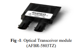
AFBR-5803Z Optical Transceiver
HFBR-1119TZ Optical Transmitter
HFBR-2119TZ Optical Receiver
RJ-45 Integrated Magnetics
A. WIZ-830MJ
WIZ-830MJ is a network Module that includes W5300 (TCP/IP Hardwired chip, include PHY), MAG-JACK (RJ-45 with transformer). It has high network performance. It operates at 3.3V
with 5V I/O signal tolerance. It includes hardware internet protocols such as TCP, IP Ver.4, UDP, ICMP, ARP, PPPoE, IGMP. It also includes hardware Ethernet protocols such as DLC, MAC.
B. EP1C12 FPGA
The flexibility and reconfigurability of FPGAs makes them an ideal solution for systems that demand a diverse set of high-speed I/O requirements. Along with the high-speed I/O
capabilities, the FPGAs provide millions of configurable gates, lots of on-chip static memory, and additional dedicated system resources such as processor cores, phase-locked loops (PLLs), digital signal processing (DSP) blocks, PCI Express® (PCIe®) channels
C. WIZNET W5300 CHIP
WIZnet chip W5300 contains the technology of full hardware logic of communication protocols such as TCP, UDP, IPv4, ICMP, IGMP, ARP and PPPoE. In order to provide high performing data communication, the data communication memory is extended to 128kbyte and a 16bit bus interface is supported in W5300. Users can utilize 8 independent hardware SOCKETs for
high-speed data communication.
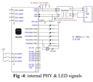
If the internal PHY does not satisfy the user’s requirements, an external PHY made by 3 rd party can be interfaced. In case of using external PHY mode, W5300 clock source should be
selected. When TEST_MODE0 is logically high, a crystal is used, and when TEST_MODE1 is logically high, an oscillator is used.
D. DP83640 Precision PHYTER
The DP83640 is a highly reliable, feature rich device suited for industrial applications. The DP83640 offers low power consumption, including several intelligent power down states. In addition to low power, the DP83640 is optimized for cable length performance far exceeding IEEE specifications. The DP83640 includes a 25MHz clock out. This allows the application to be designed with a minimum of external parts, which in turn results in the lowest possible total cost of the solution.
E. AFBR-5803 Optical Transceiver
The AFBR-5803Z/5803TZ are 1300 nm products. The transmitter section of the AFBR-5803Z and AFBR-5805Z s-eries- utilize 1300 nm Surface Emitting InGaAsP LEDs. These LEDs are packaged in the optical subassembly portion of the transmitter section. They are driven by a custom silicon IC which converts differential PECL logic s-ignals-, ECL.
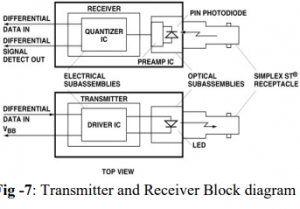
F. HFBR-1119TZ Optical Transmitter and HFBR-2119TZ Optical Receiver The HFBR-1119TZ/-2119TZ series of data links are highperformance, cost-efficient, transmitter and receiver modules for serial optical data communication applications specified at 266 MBd for Fibre Channel applications. These modules are designed for 50 or 62.5 µm core multimode optical fiber and operate at a nominal wavelength of 1300 nm [8].
IV. DESIGN
The design of the Data Transmission System using Ethernet and Fiber Optic link involves proper data flow between components whose control logic is designed in FPGA. The signals
coming out from the measurement control system are sent to data transmission system via fiber optic cable which is received by optical transceiver. The optical transceiver consists of in
built transmitter and receiver module. Hence the receiver receives the optical signal and convert it into an electric signal, and then extract the clock and recover the data. The output signal from receiver is fed to the external PHY chip DP83640 which is interfaced with optical Transceiver AFBR-5803Z. This chip then converts the received signal into equivalent 4 bits i.e; nibble wide data signal by using 100 Base-FX Receive logic employed in the chip.
V. SYSTEM SOFTWARE PART
The software implementation of the Data Transmission System is based on the Quartus II development Environment using top-down design ideas. The FPGA logic is written using Verilog code. For communication to take place between host computer and data transmission system we are using W5300 as the Ethernet controller. There are two methods to establish connection one is TCP-SERVER mode that is waiting for connection request. The other is TCP-CLIENT mode that sends connection request to a server. W5300 has total of eight SOCKETS each of which can be configured independently. When communication is established only one socket is active.
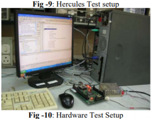
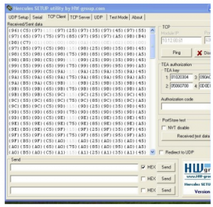
VI. CONCLUSION
The complete circuit schematics of Data transmission System is designed using Protel 99SE software tool according to PCB component placement with FPGA as the master control unit. The use of Fiber optic link in the system, transfer the data at a very high speed with negligible loss. Also the data can be transferred up to several kilometers without having to worry about losses. The program design of the proposed data transmission system based on the Verilog is detailed. The debugging of the test code is done with Quartus II development environment and it is tested on the FPGA board. The Test results shows that the data Transmission System program can be feasible and the Data Transmission System can be look as the bridge between the host computer and the measurement control system.
COMMENTS